
Concept explainers
Videos
Each diode cut−in voltage in the circuit in Figure P2.59 is 0.7 V. Determine
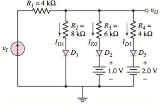
Figure P2.59
(a).
The values of
Answer to Problem 2.59P
Explanation of Solution
Given Information:
The given circuit is shown below.
Calculation:
For
The input voltage is dropped across the output because the current in the circuit is zero.
(b).
The values of
Answer to Problem 2.59P
Explanation of Solution
Given Information:
The given circuit is shown below.

Calculation:
For
The value of diode current
The modified circuit is:
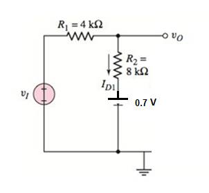
Applying Kirchhoff’s voltage law:
The value of output voltage
(c).
The values of
Answer to Problem 2.59P
Explanation of Solution
Given Information:
The given circuit is shown below.

Calculation:
Assuming the diodes are in forward bias and in active mode.
Applying Kirchhoff’s current law at output node:
From above calculation diodes D1,D2 are in forward bias active mode but the diode D3 is in cut off mode because the voltage difference between positive and negative terminal is less than 0.7 V. The current through diode D3 is zero.
Hence, the assumption is incorrect.
The modified figure is:
Applying Kirchhoff’s current law at output node:
The diode currents
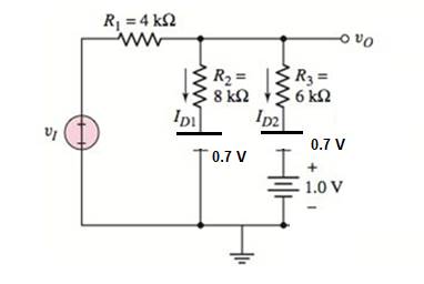
(d).
The values of
Answer to Problem 2.59P
Explanation of Solution
Given Information:
The given circuit is shown below.

Calculation:
For
Applying Kirchhoff’s current law at output node:
The values of diode currents are:
Want to see more full solutions like this?
Chapter 2 Solutions
Microelectronics: Circuit Analysis and Design


- For the circuit shown in the Figure, if the diodes are silicon diodes with Vp(on)=0.7 V, and VIN=50 sin wt V, V1 =6 V and V2 = 16 V, then the value of VouTP-p) is: R, D VaN Vout v1事 2章 Oa. 25.4 V Ob. 27.4 V Oc. 29.4 V Od. 23.4 Varrow_forwardFor the circuit below, assume the diodes operate with a constant voltage drop of .7V, find Vx, Vy, VD4 and ID2. 15V 15V Allt V1 V2 R1 1k IDC 1mA Vx R2 2k ww D1N4002 Vy D1N4002 7D1 D1N4002 D2 D3 R3 1k D4 D1N4002arrow_forwardGiven the following circuit with VDD= 9.2 V, R=2.3 k2, then the current Iis: Use the CVD model for the diode, with VD = 0.65 V. I VDD a. 0.004000 A O b. 3.717391 A OC. 0 A d. 4.000000 A e. 0.003717 A R + VD -arrow_forward
- In the circuit given in the figure, find the current passing through the diode in mA since R1 = 4.95Kohm, R2 = 2.50Kohm, R3 = 1.69Kohm, R4 = 5.44Kohm, VCC = 13.00V and the diode is silicon?arrow_forwardQ2:- Find the level of Vo for each circuit shown in the Figure below. Also, determine the status of each diode; if it is forward or reverses biasing. Assume all diodes are silicone with 0.7v drop. +5 V +15 V -10 V (12 Marks) R DI +5 VoK D +5 VoK DI -5 VoH -5 Vo4 D2 D2 D2 +5 VoH D3 +5 Vo4 D3 -10 VoK D4 V. -5 Vo K (a) (b)arrow_forwardConsider the circuit in figure 2. Diode D1 is germanium and D2 is gallium arsenide. Determine the following: a. The states of D1 and D2. Explain. b. Current I1 through R1 c. Current I2 through R2 d. Current I3 through R3 e. Voltage across R1 f. Voltage across R2 g. Voltage Across R3arrow_forward
- 2. Figure A.1 shows I-V characteristics of two diodes, namely A and B. Diode A has higher dynamic resistance than diode B. UTM &UT ID 4 5UTM 3TM UTM UTM &UTM 5 UTM & UTM UTM 3 UTM 03 TM 6 UT 0.68 (a) UTM VD Figure A.1 State one possible reason why the diodes have different knee voltage values. UTM OM & UTM 3 UTM & TM (b) Based on Figure A.1, identify the knee voltage of UTM" TM 5 UTde BE UTMarrow_forwardAll pn diodes shown below have a voltage drop of 0.3 V when they are "ON". +4V DIA 5k2 D2 VOUT VA 5k2 V8 D1B -2V Indicate in the table whether the diodes D1A, D1B and D2 are ON/OFF with the given VA and VB values. Also give the corresponding VOUT numerical values. DIA (ON/OFF) DiB(ON/OFF) Dz(ON/OFF) VoUT (sign and numerical value) VA |V8 OV +4V OV +3V ov +4Varrow_forwardConsider the circuit shown in Figure 2. The cut-in voltage of each diode is . Let and assume both diodes are conducting. Determine if this is a valid assumption and explain your answer. And calculate the values of IR, ID, Ip2, and V.. Rj =1.7 kQ ww VB =1 V D1 Dz R2D 4 kQ Figure 2arrow_forward
- liting Q9. For the circuit shown in Figure C9, Calculate the following i) Current through the Silicon diode (Isi). ii) Current through the Resistor R2 (1). iii) Current through the diode D4 (IGe4). iv) Voltage at points V3 and V4. Is D1. D2 Si Si oV4 RI 1.3K2 R3 2.7K R2 3K2 IGe4| 15V D5 Si 03 D4 Ge Ge V2 1V Figure C9arrow_forwardFor the circuit shown in the Figure, if the diodes are silicon diodes with VD(on)=0.7 V, and VIn=50 sin wt V, V1 =7 V and V2 =13 V, then the value of VOUT (p-p) is: R1 D, D2 VIN VOUT vi E v2= Ca. 19.4 V Ob. 17.4 V Cc. 15.4 V Cd. 21.4 Varrow_forward(a) State one possible reason why the diodes have different knee voltage values. 2. Figure A.1 shows I-V characteristics of two diodes, namely A and B. Diode A has UTM higher dynamic resistance than diode B. 5 UTM U UTM Ip UTM TM 3 UTM UTM O UTM UTM UTM UTM & UTM 03 TM UTM 0.68 VD Figure A.1 State one possible reason why the diodes have different knee voltage values. 5 UTM & UTM M 3 UTM (b) Based on Figure A.1, identify the knee voltage of UTM (c) Draw with complete labelling an equivalent circuit that represents the circuit in UFigure A.2. Consider practical diode model. TM 5 UTM 5 UPde BE UTM & UTM & UTM 1 ΚΩ Diode B 5 UTM O UTM UTM & UTM & UTM 1.5 V 5 UTM UT 5 UTM 3 V 5 UTM O UTM Figure A.2 M G UTM 5 UTM 5 UTM & UTM 5 UTM UTMarrow_forward
