
Concept explainers
Videos
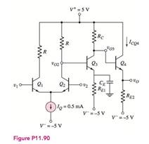
Consider the multistage bipolar circuit in Figure P 11.90, in which de base currents are negligible. Assume the transistor parameters are
(a)
The design parameters for the circuit.
Answer to Problem 11.90P
The value of the resistances to design the circuit is
Explanation of Solution
Given:
The given diagram is shown in Figure 1
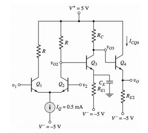
Figure 1
The given values are
Calculation:
The collector for both the transistors are equal and is given by,
The expression for the voltage
Substitute
The value of the voltage
The value of the resistance
The value of the resistance
The value of the resistance
Conclusion:
Therefore, the value of the resistances to design the circuit is
(b)
The value of the differential mode voltage gain
Answer to Problem 11.90P
The value of the differential voltage gain is
Explanation of Solution
The given diagram is shown in Figure 1

Figure 1
Calculation:
The expression for the gain
The value of the gain
The value of the resistance
The value of the gain
The value of the gain
The value of the voltage gain
Substitute
Conclusion:
Therefore, the value of the differential voltage gain is
(c)
The value of
Answer to Problem 11.90P
The values of the gain are
Explanation of Solution
The given diagram is shown in Figure 1

Figure 1
Calculation:
The value of the voltage
The value of the common mode voltage
Solve further as,
The value of the common mode rejection ration is calculated as,
Conclusion:
Therefore, the values of the gain are
Want to see more full solutions like this?
Chapter 11 Solutions
Microelectronics: Circuit Analysis and Design


- 1. Draw the equivalent circuit and the model in AC mode. 2. Specify the type of transistor and the basic configuration of the circuit. 3. Find the voltage gain and output voltage, with = 300 and Ap(db) =47. 4. We add to this circuit an internal resistance (R₂) of 50052: 4.1. Draw the new circuit with R 4.2. What is the new output voltage, with r' = 250? 4.3. Determine the power gain if A₁ = 41.94 db - Vee 15V 5mV La 20 2 4.4 k 6.3 k 20 16 karrow_forwardFor the 2 circuits shown above, βnpn = 100, βpnp = 50, VDO = 0.7 V, R2 = 150 kΩ, and RB = 12 kΩ Using the ac small-scale signal analysis, determine for each circuit: a) The voltage gain (Av = vout/vin) b) The input resistance (Rin) c) The output resistance (Rout)arrow_forwardQ2) for the amplifier shown in Figure 1) Determine the voltage gain (Av) and the current Gain (Ai) 2) Determine The input and output resistance 3) Determine The output voltage Vout 4) Draw The Ac load line 5) Draw the AC equivalent circuit 6) Determine the maximum input voltage (Vi(p-p)) for maximum output voltage (Vo(p-p)) without distortion. HH Vi-20 mv RB 56 kQ +₁ D B = 50 - 10 V HH RE 1kQ Vou RL • 10 Ω ww11arrow_forward
- 4. For the transistor in the figure shown below, the parameters are ß = 100 and VÀ = ∞. a. Design the circuit such that lEQ = 1mA and the Q-pt is in the center of the dc load line. b. If the peak-to-peak sinusoidal output voltage is 4V, determine the peak-to-peak sinusoidal signals at the base of the transistor and the peak-to-peak value of Vs. If the load resistor R₁ = 1kQ is connected to the output through a coupling capacitor, determine the peak-to-peak value in the output voltage, assuming vs is equal to the value determined in part (b). Vcc=+10 V www Rs = 0.7 kΩ Cc www RB RE voarrow_forwardFind the parameters from this circuit Parameters ..beta , re , IEQarrow_forward1. Draw the small-signal equivalent circuit and derive the input resistance of the bipolar transistor circuit below: Vcc RL RB RE VBBarrow_forward
- In the circuit shown in Figure 1, the input signal vsig is a small sine-wave signal with zeroaverage. The transistor β is 100.Figure 1: BJT Amplifier(a) For RL = 10KΩ, draw the small-signal equivalent circuit of the amplifier and determineits overall voltage gain.(b) What is the input resistance of the amplifier circuit?arrow_forwardI think is true because the Wilson circuit provide a high output resistances , is it true or false and whyarrow_forwardDraw the DC and AC load line for a transistor amplifier circuit shown in Figure, also describe the optimum operating Point for the given values as follows: Rc = 10 KQ ; RL=20 KQ and V cc = 20 V +Vcc Ic Rc Cc Cc V. out R1 Vin wwwarrow_forward
- V* = + |ov Ri Rip ERC Vs RE V: -sV The following parameters are given for this transistor: B = 200 and VA = o. Design the circuit with the following value ICQ = 1.5mA and VCEQ = 5V. Find the small signal voltage gain AV = Vo/Vs. Find the input resistance in the signal source Vs.arrow_forwardDetermine the ac parameters for this BJT circuit. Note: DC biasing voltages and currents need to be computed FIRST before calculating the AC parameters of gains and impedances 80 mV HI +10 V R₁ 18 ΚΩ R₂ > 4.7 ΚΩ Rc • 1.5 ΚΩ hFE = 30 hfe = 200 RE * 1.2 ΚΩ CE RL > 5.1 ΚΩarrow_forwardConsider the circuit shown in figure, where VBE=710 mV, B = 100, and VA = co. Calculate the Vc of Q1. Assume that the emitter current is equal to collector current. al Circuit parameters / Rg = 20 kn, Rc = 300 N, Rɛ = 500 N, Vcc = 3 V Vcc RB Rc REarrow_forward
 Introductory Circuit Analysis (13th Edition)Electrical EngineeringISBN:9780133923605Author:Robert L. BoylestadPublisher:PEARSON
 Delmar's Standard Textbook Of ElectricityElectrical EngineeringISBN:9781337900348Author:Stephen L. HermanPublisher:Cengage Learning
 Programmable Logic ControllersElectrical EngineeringISBN:9780073373843Author:Frank D. PetruzellaPublisher:McGraw-Hill Education
 Fundamentals of Electric CircuitsElectrical EngineeringISBN:9780078028229Author:Charles K Alexander, Matthew SadikuPublisher:McGraw-Hill Education
 Electric Circuits. (11th Edition)Electrical EngineeringISBN:9780134746968Author:James W. Nilsson, Susan RiedelPublisher:PEARSON
 Engineering ElectromagneticsElectrical EngineeringISBN:9780078028151Author:Hayt, William H. (william Hart), Jr, BUCK, John A.Publisher:Mcgraw-hill Education,