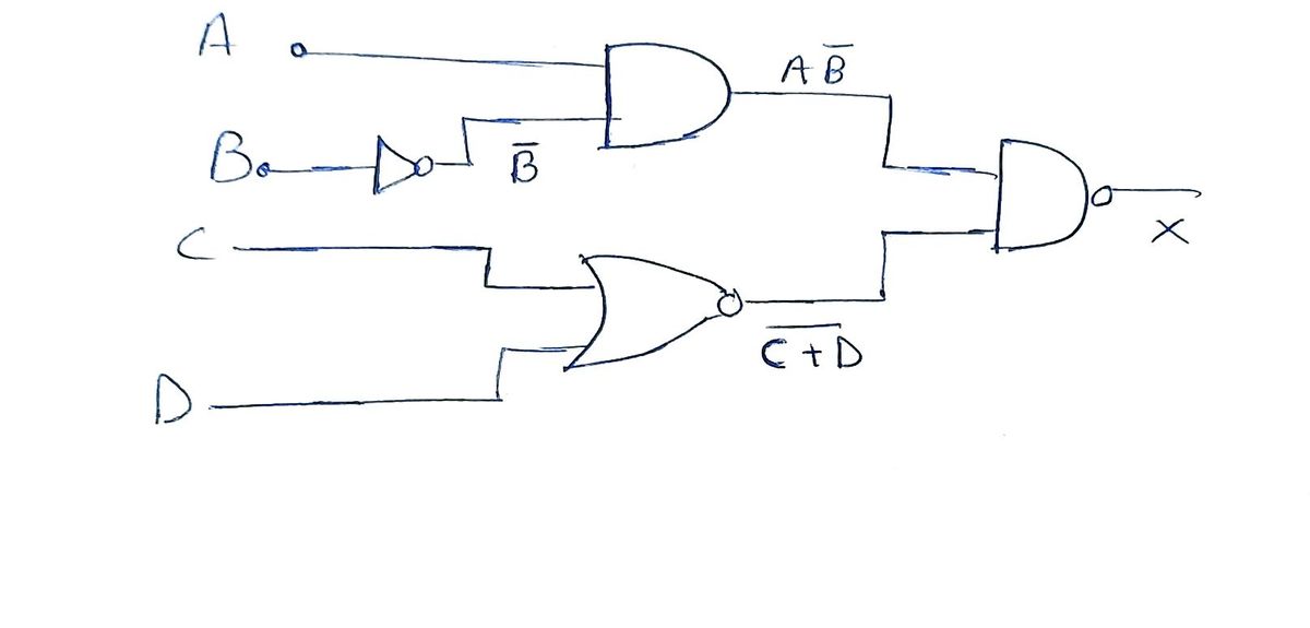
6. Using your NAND chips, build the following logic circuit. Using the truth table below, determine what the expected output should be then carry the circuit through its truth table and see how well the circuit operation matches your expectations. A B C What is the Boolean expression for this circuit? D X= Input Input Input Input Expt'ed Actual Input| Input Input | Input| Expt'ed Actual А B C D A B C
Q: design a logic circuit that accepts decimal input for a 4 bit full adder subtractor with truth table…
A: We need to design a logic circuit that accepts decimal input for a 4-bit full adder subtractor.…
Q: 18. Derive the Boolean expression for the logic circuit below: a. CA + CB +CD A B b. C(A + B)D с.…
A:
Q: Q: Refer to the state assigned table shown below, by using Moore model, design a logic circuit for…
A:
Q: Simplify the given expression to its SOP form. Draw the logic circuit for the simplified SOP…
A:
Q: For the logic equation Q = AB+ CD’ , to make the output 1, which values of the inputs A, B, C, D…
A:
Q: 1.2 For the given Boolean expression below, implement the logic circuit without simplifying it.…
A:
Q: a) Obtain the Truth table for the given Logic Expression with intermediate outputs. X=(AB +BC) + c…
A: Given expression is X=(AB+BC) +cbar
Q: F(A, B, C, D) = E(0, 2, 8, 9, 10, 11, 15) with d(A, B, C, D)= E(4, 6, 12, 13) 1) Given the Boolean…
A:
Q: ) Logic Function F (x, y, z, w) = ∑ m (0,2,4,6,10,13) + ∑ k (8,12) as sum of minimers is given a)…
A:
Q: 1.2 For the given Boolean expression below, implement the logic circuit without simplifying it.…
A:
Q: 1. The expression F (A, B, C) = E (0,2,5,6,7) a. Draw the truth table b. Generate the Karnough map…
A:
Q: 2) Design a logic circuit to realize the following Boolean function F(x,y,z) = IIM(0,1, 2, 6, 7) D)…
A: 1.Decoder
Q: Simplify the following Boolean expression after that you will have to draw a logic circuit for the…
A:
Q: Use De Morgan's Theorem for ((a' + bc)d' + e )' Create the logic diagram of the simplified function
A: In this question, we have to realize the function usingde morgans theoremThe function is given…
Q: For the logic equation Q = AB+ CD' , to make the output 1, which values of the inputs A, B, C, D…
A:
Q: Q;: Refer to the state assigned table shown below, by using Moore model, design a logic circuit for…
A: The given state table can be modified as,
Q: 3- Obtain a digital network with output F that will produce a logic 1 (F-1) when a 4-bit binary…
A:
Q: (a) From the expression X ( (AB*C+(AB)*)*+ABC) where * indicates the complement (i) Draw the logic…
A: A (1): The given expression is: X = (AB'C + (AB)']' + ABC X = (AB'C)' . AB + ABC X = [(AB')' + C']…
Q: Q2: (a) Design a two-input magnitude comparator, write the truth table, simplify and draw the logic…
A: Design a two-input magnitude comparator, write the truth table, simplify and draw the logic circuit
Q: Design a combinational logic circuit that converts a three-bit binary number from code A to code B,…
A: The solution for the given problem is given below.
Q: Given the Boolean expression a’b + a’c’ + abc, a. Convert the expression to the other standard form.…
A: Brief description: For the given Boolean expression a’b + a’c’ + abc, we need to write SOP & POS…
Q: a. Fill in the Karnaugh map for the logic functiondefined by the truth table.b. What is the minimum…
A: To find the Karnaugh map for the logic function using given truth table is shown as:
Q: For the given Boolean function: F = ABC+ABD+A’BCD’+AB’C’+B’CD i) Find the minimal Sum of Product…
A:
Q: Design a PLA circuit which realizes the following Boolean functions: "check the image" (a) Simplify…
A:
Q: A logic family has a power-delay product of 100 fJ.If a logic gate consumes a power of 100 W,…
A: Given: PDP= 100 fJP= 100 μW
Q: Logic Function F (x, y, z, w) = ∑ m (0,2,4,6,10,13) + ∑ k (8,12) as sum of minimers are given.…
A: Ans (a) Truth table
Q: A function F is defined including Don’t Care by: F (A.B, C, D) = Em( 0, 2, 3, 5, 6, 7, 8, 9) +…
A:
Q: The expression of a logic circuit whose output is X is given below. Find the simplified POS…
A:
Q: Design a combinational logic circuit that converts a three-bit binary number from code A to code B,…
A: Redraw the truth table. Inputs (Code A) Outputs (Code B) A2 A1 A0 B2 B1 B0 0…
Q: 4. The truth table of a logic operation is given at the right- hand side. A В C Y 1 (a) Derive the…
A:
Q: Write the Boolean equation and draw the logic diagram of the circuit whose outputs are defined by…
A:
Q: Design a combinational logic circuit whose input is a four-bit number and whose output is the 2's…
A: Combinational circuit: It is a digital circuit and its output is dependent on the combination of the…
Q: a. Construct a Karnaugh map for the logic function F = A ¯ B C ¯ D ¯ +AB C ¯ D ¯ + A ¯ B C ¯ D +AB C…
A: The above function is given as K-map is given as
Q: AAo 00 9. AIAO A3A> 01 %3D 10 A3A 00 00 00 16 10 b= A3 A, Ao + A3 AIAO
A: Given the K-map and truth table of the combinational circuit. We need to design the combinational…
Q: 11. Design a simple circuit from the function by reducing it using appropriate k-map, draw…
A:
Q: Determine the minimum Boolean expression for the logic circuit shown below. A B O 1) A B+ A.B O 2)…
A: Given circuit:
Q: Determine the minimum Boolean expression for the logic circuit shown below. A B C O 1) A B+ A B O 2)…
A: Given circuit,
Q: Answer this question, part (3). Design a combinational logic circuit that converts a three-bit…
A: The solution is attached below for the given problem.
Q: . Simplify the Boolean expression AB+(AC)`+AB`C(AB+C) 5. Use the Design Procedure to design a…
A: “Since you have asked multiple questions, we will solve the first question for you. If you want any…
Q: Task 3: Digital logic circuit analysis - Finding the Boolean expression of a given circuit Find the…
A: Redrawing the circuit by applying the input as shown below:
Q: 5. (a) Simplify the Boolean expression and draw the logic diagram that implements the simplified…
A: Explanation is given in the successive step
Q: Design a logic circuit using two 2-to-4 decoders to realize the following Boolean function F(A,B,C)…
A: We will Design the given Boolean expression by using of decoder and OR gate .
Q: design logic circuit of MODE 6 counter that count {7 3 1 5 3 0} use JK flip flop in your design?
A:
Q: Example3 Write a Boolean expression for this truth table, then simplify that expression as much as…
A:
Q: Given f (w, x, y, z) = II(0, 1,3, 5, 13), a) Write the complete truth table for Y = f(w, x, y, z).…
A:
Q: In this exercise, you will be creating a 4-variable K-map to minimize the logic for the truth table…
A:
Q: Q. If the the given Boolean Function, F(A, B, C, D) = E(1,4, 8, 9, 10, 11, 12, 14). is reduced using…
A: The SOP form is a method of simplifying the Boolean expressions of logic gates. In this SOP form of…
Q: C 10 11 4X1 12 Q MUX F(A,B,C,D) 13 S1 SO A = MSB D = LSB %3D A B Which of the following is the…
A:
Q: Given the Logic Circuit above, fill-up the truth table below.
A: NAND GATE A B Output 0 0 1 0 1 1 1 0 1 1 1 0 EXOR GATE A B Output 0 0 0 0 1…
Trending now
This is a popular solution!
Step by step
Solved in 3 steps with 3 images
- 3-) Analyze the circuits below and write the Boolean equation for each Part. Simplify the equation using Boolean algebra and determine if they function as an XOR, XNOR or neither. A): Dor B): XD XD . D3. Design and Show the connection on the circuit that would add two 6-bit data, D: (D6 Ds Di) and H: (H6 Hs Hi). You may use 4-bit adders. Draw the circuit and clearly indicate/identify all input and outputs. Show addition of Ds to Hs and Sum (Es). Do not draw switches, resistors, and LEDS at inputs or outputs. 7483A 7483A A. A, A, A1 B. B. B, B, B. B. B, C, C. C. C. B,- The proportional distribution of A, B, C, D signals is given in the table as a percentage. It “logic 1” when the signals are accepted as active, “logic 0” when they are accepted as passive. takes. - When the proportional sum of active signals is over 50%, its output is "logic1", When we accept "logic 0" when it is below 50%, the output in the table Find the values. - Create an X function based on the logic values you find. Simplify the created X function. - Design the simplified function with NAND and NOR gates. - Set up the circuits you designed with NAND and NOR gates and observe the outputs. Show the output values by drawing a table, applying all possibilities to the input values.
- - The proportional distribution of A, B, C, D signals is given in the table as a percentage. It “logic 1” when the signals are accepted as active, “logic 0” when they are accepted as passive. takes. - When the proportional sum of active signals is over 50%, its output is "logic1", When we accept "logic 0" when it is below 50%, the output in the table Find the values. - Create an X function based on the logic values you find. Simplify the created X function. - Design the simplified function with NAND and NOR gates.Excess-3 code is significant for arithmetic operations as it overcomes shortcoming encountered while using 8421 BCD code to add two decimal digits whose sum exceeds 9. Excess-3 arithmetic uses different algorithm than normal non-biased BCD or binary positional number system. An electronics company has hired your services to design a code converter that converts Binary Coded Decimal (BCD) code for it. Design the converter.3. Discussion: 1. Compare between BCD code & Excess-3 code? 2. What is the reason of inventing Excess-3 Codes? 3. Find the Excess-3 code of (83.67)10 and show your work? 4. Find the decimal number of (11110001101010)Excess-3 and show your work? 5. What is the Excess-3 code of (100100001111001)BCD ? Show and verify yourwork.
- Direction: Analyze the given circuit and find the following: Logic Expression Simplified Logic Expression using Boolean Algebra Simplified CircuitDesign a combinatorial circuit that will be able to detect prime numbers given as input in binary. The input to the system will be any 4 bit binary number. The output of the circuit should be a single bit that will be 1 (high) if the input is a prime number and 0 (low) if the input is not a prime number. For example, if the input to the circuit is 0101 the output should be 1. Again if the input is 1010, the output should be 0.Q1: Design and implement an asynchronous counter that counts from 0000 up to 1100 (modulus 13). Use OR gate, and show in the drawing how the OR gate is connected to truncate the state 1101.
- To display the hexademical value of a 4- bit number on a 7-segement display. the LEDs of the seven segment compnent are lit with a logical "0" (actice low). The inputs are (active high). a) complete the below truth tablee for each output b) Using Karnaugh map provide the simplifed expession for each output(a,b,c,d)1. Gray code to Binary converter: Gray code is one of the codes used in digital systems. It has the advantage over binary numbers that only one bit in the code word changes when going from one number to the next. (See Table 1). Design a combinational circuit with 4 inputs and 4 outputs that converts a four- bit gray code number into an equivalent four-bit Binary number. Use Karnaugh map technique for simplification. Use LogicWorks for pre-lab demonstrations. Select the library "7400dev.clf* in the Parts Palette and then select the XOR chip 74-86. This would give you a set of 4 XOR's as shown in Fig. 1, just like the hardware chip 74-86. You could use as many as needed from these XOR gates in your design. Get back to ALL LIBRARIES and select switches for the inputs and Binary Probes as indicators of the outputs. Verify your design in the pre-Lab. During the Lab construct the circuit and verify its operations.Design a digital circuit using only 4-to-1 multiplexers, allowing represent the following Boolean function. As a restriction you can only use 4 multiplexers in size 4 to 1.